
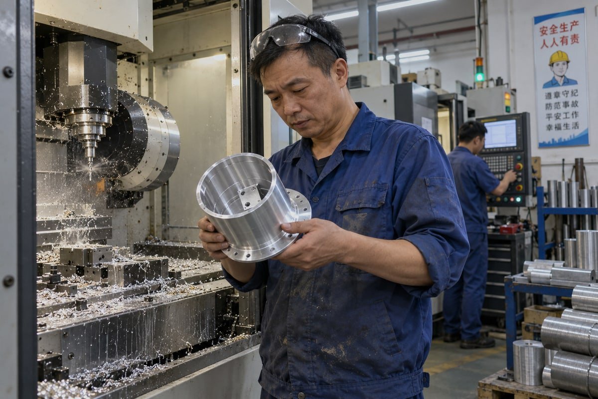
A wafer-handling bracket that drifts by a few microns can stall an entire tool. On our shop floor, CNC machining for semiconductor equipment manufacturing is about preventing exactly that.
CNC machining supports semiconductor equipment manufacturing by producing the precision parts that wafer processing equipment depends on: vacuum chamber components, gas delivery manifolds, wafer-handling arms, stage mounts, and fixtures. It delivers micron-level tolerances, controlled surface finishes, flexible material choices, and repeatable low-volume production.
Let me clear up one thing first. CNC machines do not cut transistors. They build the equipment that does. Lithography, etch, deposition, inspection, and packaging tools 1 all run on machined hardware. One more point shapes everything I write below. In this industry, supplier qualification takes a long time. Once a buyer approves a part and a shop, they rarely switch. So every choice about tolerance, material, geometry, and paperwork is a long-term choice. I will walk through those four choices one by one.
What Tolerances Can I Expect When Machining Precision Parts for Semiconductor Equipment?
Our inspection room once held a batch of stage mounts because flatness ran a few microns past the limit. Nobody argued. In semiconductor work, close enough is not close enough.
Precision tolerances for semiconductor equipment parts usually range from ±0.01 mm for structural brackets down to ±0.005 mm on critical bores, datums, and sealing faces. Some suppliers advertise ±0.0001 inch (about ±0.0025 mm), but that applies only to specific small features, not whole parts.

I want to be honest about numbers here. On our 3-axis, 4-axis, and 5-axis mills, we hold 0.01 mm as standard and 0.005 mm on features that need it. That is what our ISO 9001:2015 system is built around. I have seen shops quote ±0.0001 inch on their websites. That figure is real for a ground pin or a short bore in a stable material. It is not real for a 400 mm aluminum chamber lid in a warm workshop. Treat it as a capability claim, not an industry standard.
Tolerance by function, not by habit
The right question is not "how tight can you go?" It is "what does this feature do?" Each part type in wafer processing equipment has a different critical control.
| Part type | What really matters | Realistic tolerance focus |
|---|---|---|
| Structural frames and brackets | Stiffness, flatness, hole alignment | ±0.01 mm on mounting patterns, flatness by span |
| Vacuum chamber components | Sealing faces, parallelism, Ra | ±0.005 mm on seal lands, controlled surface finish |
| Wafer-handling end effectors | Low mass, repeatable pick position | ±0.005 mm on locating features |
| Gas delivery manifolds | Channel geometry, port position, cleanliness | ±0.01 mm on ports, burr-free passages |
| Metrology and alignment fixtures | Stability, repeatability over time | ±0.005 mm on datums, stress-relieved stock |
Why tight tolerances cost more than you think
Buyers sometimes ask us to put ±0.005 mm on every dimension "to be safe." I push back. Each tighter band adds temperature control, slower feeds, extra probing, and sometimes grinding or lapping. Scrap risk climbs too. A fit-for-purpose tolerance stack costs less and performs the same. Our DFM review flags exactly which dimensions drive the function and which can relax.
Thermal drift on large parts
Long cycles on big aluminum workpieces are a known problem. The part warms, grows, and shrinks back after cutting. Our approach is simple. We rough, let the part stabilize, then finish. On long jobs we probe in-process and compensate the offsets before the final pass. That is how a mount measures the same on our CMM and on yours.
Which Materials Should I Choose for CNC Machined Semiconductor Components?
Every quote for a cold plate forces the same choice: copper for thermal conductivity 2, or aluminum for weight and machinability. We walk customers through that trade-off almost weekly.
Choose aluminum alloys such as 6061 for lightweight frames and thermal parts, 316 stainless steel for vacuum and corrosion resistance, copper for heat transfer, PEEK or Vespel for insulating and low-particle contact parts, and ceramics or quartz where plasma exposure and high-purity materials are mandatory.

Material choice is where many semiconductor parts quietly fail. A part can measure perfectly and still outgas, corrode, or shed particles. So I look at five things before I look at price: vacuum compatibility 3, thermal behavior, chemical resistance, stiffness-to-weight, and machinability. The table below is how I explain it to engineers who send us drawings from Germany, the US, and Japan.
| Material | Strengths in fab equipment | Watch-outs in machining and service | Common uses |
|---|---|---|---|
| Aluminum 6061 / 7075 | Light, stiff enough, excellent machinability, good thermal conductivity | Needs anodizing or coating; moves with heat during long cycles | Frames, chamber lids, cold plates, end effectors |
| Stainless 304 / 316 | Strong corrosion resistance, vacuum-friendly, low outgassing | Slower to cut, work-hardens; 316 must not be swapped with 304 | Flanges, feedthrough supports, fittings |
| Copper (OFHC) | Highest thermal conductivity of the common metals | Soft, burrs easily, needs plating to stop oxidation | Heat spreaders, electrodes, cooling blocks |
| Titanium | Low mass, non-magnetic, chemically stable | Tough on tooling, higher cost | Lightweight handling arms, non-magnetic mounts |
| PEEK / Vespel | Insulating, low friction, chemical resistance, cleanroom compatibility | Higher thermal expansion, lower stiffness than metal | Wafer contact pads, insulators, grippers |
| Inconel | Keeps strength at high temperature | Very demanding to machine | Heater supports, hot-zone hardware |
| Ceramics / quartz | Plasma resistance, electrical insulation, high purity | Brittle; needs grinding or ultrasonic-assisted machining | Chamber liners, rings, plasma shields |
What we machine in-house, and what we do not pretend to
Our regular lineup covers aluminum, stainless steel, copper, brass, titanium, alloy steel, tool steel, and engineering plastics 4 including PEEK, POM, nylon, PC, PPSU, and HDPE. That covers the large majority of equipment parts we see. Ceramics and quartz are a different world. Ultrasonic-assisted machining uses high-frequency vibration to keep brittle materials from micro-cracking. That is a specialist process. If your drawing calls for alumina, I will tell you so rather than risk your part.
The material fraud problem
Buyers tell me their biggest fear is getting ordinary aluminum labeled 6061, or 304 shipped as 316. The two stainless grades look identical. They do not behave identically in corrosive process gas. Our answer is traceability. Every bar we cut for a semiconductor job carries a mill certificate 5, and that certificate ships with the parts. If you want third-party verification, ask for it at quote stage so it is built into the price.
Finish is part of the material decision
Aluminum almost always needs anodizing. Stainless usually needs passivation. Copper needs plating. These treatments change dimensions slightly. We account for that in the machining allowance. Surface finish requirements also tie back to material. A low Ra on a 316 seal face helps the O-ring seat and reduces trapped molecules that outgas under vacuum. Smooth helps. But smooth is not the same as clean, and I will come back to that.
How Can CNC Machining Handle the Complex Geometries My Semiconductor Equipment Parts Require?
A German engineer once sent us a gas manifold drawn as five welded blocks. We asked a simple question: why not machine it from one billet on our 5-axis?
CNC machining handles complex semiconductor geometries through 5-axis CNC milling, which reaches angled ports, intersecting bores, and contoured surfaces in one setup; wire EDM for sharp internal corners and thin walls; and CAM simulation plus DFM review that removes weld seams, particle traps, and unreachable features before cutting begins.

That manifold became one part. No welds to leak. No seams to trap residue. Fewer setups, so fewer stacked position errors. This is the strongest argument for CNC machining for semiconductor equipment: it turns a fragile assembly into a monolithic component. Here is the workflow we follow for complex parts.
Our seven-step path from CAD to cleanroom-ready part
- DFM review. We read the 3D model and 2D drawing together. We flag deep blind holes, thin walls, and corners that will collect particles.
- CAM programming and simulation. We check for collisions, tool reach, and chatter before any chips fly.
- Roughing and stress relief. Heavy stock removal first, then a pause so the part settles.
- 5-axis finishing. Angled gas ports, contoured surfaces, and intersecting bores get cut in one clamping.
- Wire EDM where milling cannot reach. Sharp internal corners and thin slots come off the wire, not the end mill.
- Deburring, finishing, cleaning. Burrs become particles. We remove them, then treat, then clean, then bag.
- Inspection. CMM for dimensions, surface roughness tester for Ra, and a full report.
Matching the geometry challenge to the right method
| Geometry challenge | Method we use | Why it matters for the equipment |
|---|---|---|
| Internal cooling channels in a cold plate | Deep-hole drilling plus 5-axis port machining | Even flow means even wafer temperature |
| Thin-wall vacuum chamber components | Light finishing passes, custom fixturing | Prevents distortion that breaks the seal |
| Fan-blade or impeller-style contours | Simultaneous 5-axis contouring | Smooth, continuous surfaces without blend lines |
| Cylindrical housing with a precision lens bore | Turning plus milling in one cell | Bore stays concentric to the mounting face |
| Tooling plates with alignment pins and pockets | 3-axis milling with probed datums | Pins locate wafers or dies repeatably |
Where CNC is not the answer
I will raise the objections myself. For tens of thousands of simple parts, casting or stamping beats CNC on cost. For features smaller than a tool can cut, laser processing, EDM, or microfabrication take over. And a shop with a shiny 5-axis machine but no vacuum experience is still the wrong supplier. CNC is one tool in a chain. The emerging trends prove it: isotropic superfinishing on plasma chamber parts removes directional erosion hot spots, and cryogenic machining with liquid nitrogen or CO2 produces hydrocarbon-free surfaces for EUV optics. Both sit downstream of, or alongside, the mill. We do not offer cryogenic cutting. We do make sure the part arriving at those processes is dimensionally right.
What Quality Documentation Can I Request to Ensure My Semiconductor Parts Meet Industry Standards?
The hardest lesson in twenty-plus years of exporting is this: a perfect part with no paperwork is a rejected part. Semiconductor buyers audit the record, not just the metal.
You can request a dimensional inspection report, a first article inspection (FAI) report, material certificates traceable to the mill, surface finish and treatment records, cleaning and packaging records, and an ISO 9001:2015 certificate. For vacuum parts, add leak-test or Ra measurement results.
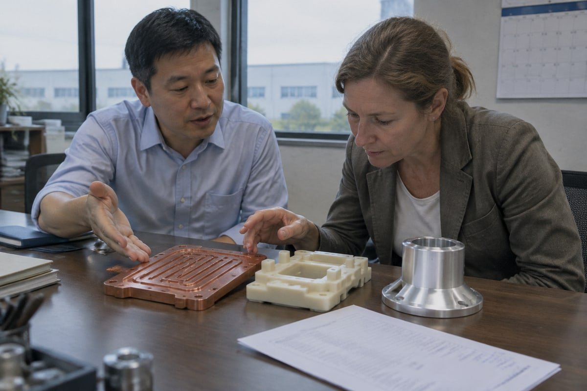
Documentation is not a formality in this industry. It is how a part gets through your incoming inspection and into a tool that costs more than our building. Here is what we provide, what each document proves, and when to ask for it.
| Document | What it proves | When to request it |
|---|---|---|
| First article inspection report | The first sample matches every drawing callout | Before approving the design for batch |
| Dimensional inspection report (CMM) | Critical dimensions on each lot are in tolerance | Every shipment, tied to lot number |
| Material certificate | Alloy grade and heat number match the drawing | Every order, especially 316 and 6061 |
| Surface finish record | Ra values on seal faces and channels | Vacuum chamber components, manifolds |
| Surface treatment record | Anodize or passivation type, thickness, vendor | Any coated or treated part |
| Cleaning and packaging record | Process used, sealed before shipping | Cleanroom-bound and vacuum parts |
| ISO 9001:2015 certificate | The quality system is audited and current | At supplier qualification |
Why the qualification cycle changes everything
Here is the insight that shapes how we run semiconductor jobs. Product qualification in this sector is long. A buyer tests samples, audits the process, runs pilot lots, then approves. That can take months. Once approved, customers do not switch suppliers lightly, because switching means repeating the whole cycle. Two things follow. First, you should choose a shop as a multi-year partner, not a one-off vendor. Second, the shop must protect that approval with boring consistency. Sample quality is easy. Batch ten, batch fifty, same dimensions, same Ra, same packaging, that is the real test. We run in-process checks against the FAI, do outgoing inspection on every lot, and back it with a 30-day warranty. If something is wrong, we rework or remake fast, because a stalled tool costs you far more than a reshipped bracket costs us.
Smooth is not clean
A low Ra does not guarantee a clean part. Cleanliness also depends on burr removal, cutting fluid residue, embedded particles, and how the part was handled after inspection. Blind holes and internal channels are the hardest to clean and the hardest to verify. So we document the deburr step and the cleaning method, and we seal parts individually before they leave Dongguan. For deliveries to Europe and North America, that packaging record matters as much as the CMM printout. If your incoming inspection needs a specific format for any of these documents, send it with the RFQ. We will match it.
Conclusion
Unstable parts stall expensive tools and burn qualification time. CNC machining prevents that when precision tolerances, the right materials, 5-axis capability, and full documentation arrive together, batch after batch.
Footnotes
1. Global industry association representing the semiconductor manufacturing equipment and materials supply chain. ↩︎
2. Scientific explanation of the physical property governing heat transfer in semiconductor cooling components. ↩︎
3. Professional society providing resources on vacuum science and material compatibility for semiconductor environments. ↩︎
4. Technical overview of high-performance polymers used for their mechanical and thermal properties. ↩︎
5. Authoritative standards organization providing guidelines for material quality and mill certification traceability. ↩︎

 English
 Italiano
 Français
 日本語
 Deutsch (Sie)
 Español
 Русский
 العربية
 Български
 Čeština
 Dansk
 Suomi
 עִבְרִית
 हिन्दी
 Nederlands
 Português
 Română
 Slovenčina
 Svenska
 ไทย
 Tiếng Việt
 Türkçe
 Slovenščina